


Research
Keywords
- Superconductivity
- Magmetism
- Layered materials
- Chiral materials
- Strongly correlated electrons
Subject
Superconductors and magnets, novel materials synthesis, layered materials,
transition metal dichalcogenides, van der Waals heterostructure, material
characterization, thin flake devices, thin film, MBE, TEM
Outline
Synthesis of new crystals without inversion symmetry
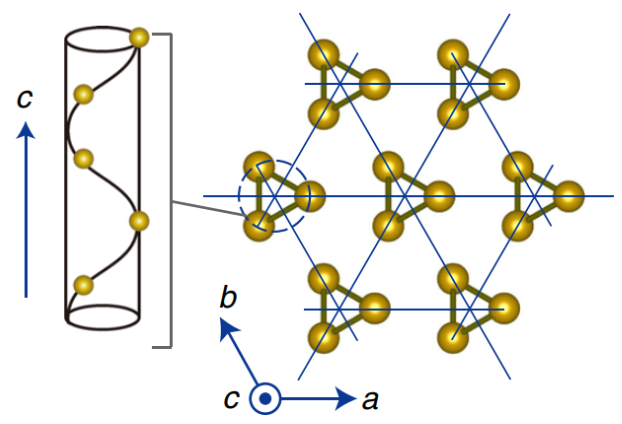
Symmetry is one of the fundamental concepts in understanding electronic properties of materials. When inversion symmetry is broken, lifted band degeneracy triggers intriguing phenomena. One outstanding example of crystal without inversion symmetry is that with chiral crystal structure. Figure 1 depicts the Te chiral network of elemental Te. The chiral chains exhibit either right- or left-handed chirality. The spin distribution at the Fermi surface differs depending on the crystals structure, leading it to the opposing response to the current.
Metastable crystal structure and unique electronic properties
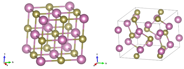
Materials can exist in several polymorphs while maintaining the same chemical formula. High pressure during synthesis helps stabilize metastable states. Chalcogenides exhibit a variety of crystal structures, even in binary compounds. For example, InTe adopts a tetragonal crystal structure and appears as a white semiconductor. Under high pressure and high temperature, it transforms into a rock salt structure and becomes a metal with a shiny black surface. These extreme conditions further expand the accessible phase space in doped topological crystalline insulator SnTe.
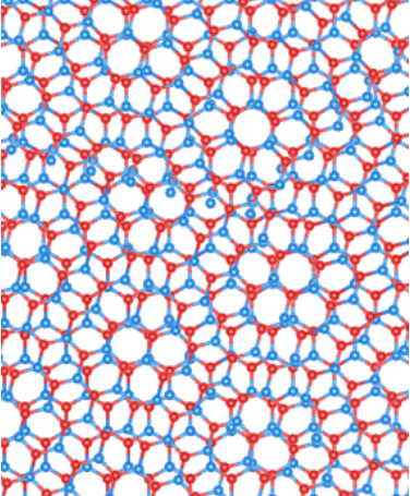
Metastability also occurs in layered dichalcogenides. For example, TaSe₂ can adopt multiple polytypes depending on the chalcogen configuration around Ta, as well as the stacking sequence of TaSe₂ layers. Even a slight change in stacking sequence can enhance the superconducting transition temperature.
Young students as well as those who are interested in aforementioned research fields are welcome to visit at our Lab. and to have discussions with us.
Recent Highlights
- T. Furukawa, Y. Shimokawa, K. Kobayashi, T. Itou,
Nat. Commun. 8, 954 (2017).
DOI: https://doi.org/10.1038/s41467-017-01093-3 - Kaya Kobayashi, Yukio Ai, Harald O. Jeschke, and Jun Akimitsu
Phys. Rev. B 97, 104511 (2018).
DOI: https://doi.org/10.1103/PhysRevB.97.104511 - Yuki Tanaka, Hideki Matsuoka, Masaki Nakano, Yue Wang, Sana Sasakura, Kaya Kobayashi, and Yoshihiro Iwasa,
Nano Letters, 20 (3) 1725-1730 (2020).
DOI: https://doi.org/10.1021/acs.nanolett.9b04906
Staff
-
 KOBAYASHI KayaProfessorEmailkayakobayashi(at)es.hokudai.ac.jpOffice03-101
 -
 OISHI RyoheiAssistant ProfessorEmailoishi(at)es.hokudai.ac.jpOffice03-103
 -
 KONDO KenjiAssociate ProfessorEmailkkondo(at)es.hokudai.ac.jpOffice03-102-1
Contact
ZIP Code 001-0020
Address Kita 20, Nisi 10, Kita-ku, Sapporo 060-0810, JAPAN
TEL +81(JPN)-11-706-9423
FAX +81(JPN)-11-706-9427